
In previous chapter, we discussed the four flip-flops, namely SR flip-flop, D flip-flop, JK flip-flop & T flip-flop. We can convert one flip-flop into the remaining three flip-flops by including some additional logic. So, there will be total of twelve flip-flop conversions.
Follow these steps for converting one flip-flop to the other.
- Consider the characteristic table of desired flip-flop.
- Fill the excitation values (inputs) of given flip-flop for each combination of present state and next state. The excitation table for all flip-flops is shown below.
| Present State | Next State | SR flip-flop inputs | D flip-flop input | JK flip-flop inputs | T flip-flop input | ||
|---|---|---|---|---|---|---|---|
| Q(t) | Q(t+1) | S | R | D | J | K | T |
| 0 | 0 | 0 | x | 0 | 0 | x | 0 |
| 0 | 1 | 1 | 0 | 1 | 1 | x | 1 |
| 1 | 0 | 0 | 1 | 0 | x | 1 | 1 |
| 1 | 1 | x | 0 | 1 | x | 0 | 0 |
- Get the simplified expressions for each excitation input. If necessary, use Kmaps for simplifying.
- Draw the circuit diagram of desired flip-flop according to the simplified expressions using given flip-flop and necessary logic gates.
Now, let us convert few flip-flops into other. Follow the same process for remaining flipflop conversions.
SR Flip-Flop to other Flip-Flop Conversions
Following are the three possible conversions of SR flip-flop to other flip-flops.
- SR flip-flop to D flip-flop
- SR flip-flop to JK flip-flop
- SR flip-flop to T flip-flop
SR flip-flop to D flip-flop conversion
Here, the given flip-flop is SR flip-flop and the desired flip-flop is D flip-flop. Therefore, consider the following characteristic table of D flip-flop.
| D flip-flop input | Present State | Next State |
|---|---|---|
| D | Q(t) | Q(t + 1) |
| 0 | 0 | 0 |
| 0 | 1 | 0 |
| 1 | 0 | 1 |
| 1 | 1 | 1 |
We know that SR flip-flop has two inputs S & R. So, write down the excitation values of SR flip-flop for each combination of present state and next state values. The following table shows the characteristic table of D flip-flop along with the excitation inputs of SR flip-flop.
| D flip-flop input | Present State | Next State | SR flip-flop inputs | |
|---|---|---|---|---|
| D | Q(t) | Q(t + 1) | S | R |
| 0 | 0 | 0 | 0 | x |
| 0 | 1 | 0 | 0 | 1 |
| 1 | 0 | 1 | 1 | 0 |
| 1 | 1 | 1 | x | 0 |
From the above table, we can write the Boolean functions for each input as below.
We can use 2 variable K-Maps for getting simplified expressions for these inputs. The k-Maps for S & R are shown below.
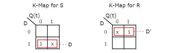
So, we got S = D & R = D' after simplifying. The circuit diagram of D flip-flop is shown in the following figure.
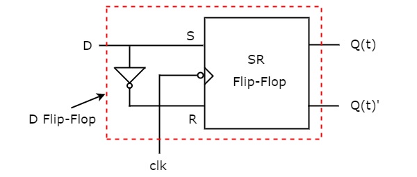
This circuit consists of SR flip-flop and an inverter. This inverter produces an output, which is complement of input, D. So, the overall circuit has single input, D and two outputs Q(t) & Q(t)'. Hence, it is a D flip-flop. Similarly, you can do other two conversions.
D Flip-Flop to other Flip-Flop Conversions
Following are the three possible conversions of D flip-flop to other flip-flops.
- D flip-flop to T flip-flop
- D flip-flop to SR flip-flop
- D flip-flop to JK flip-flop
D flip-flop to T flip-flop conversion
Here, the given flip-flop is D flip-flop and the desired flip-flop is T flip-flop. Therefore, consider the following characteristic table of T flip-flop.
| T flip-flop input | Present State | Next State |
|---|---|---|
| T | Q(t) | Q(t + 1) |
| 0 | 0 | 0 |
| 0 | 1 | 1 |
| 1 | 0 | 1 |
| 1 | 1 | 0 |
We know that D flip-flop has single input D. So, write down the excitation values of D flip-flop for each combination of present state and next state values. The following table shows the characteristic table of T flip-flop along with the excitation input of D flip-flop.
| T flip-flop input | Present State | Next State | D flip-flop input |
|---|---|---|---|
| T | Q(t) | Q(t + 1) | D |
| 0 | 0 | 0 | 0 |
| 0 | 1 | 1 | 1 |
| 1 | 0 | 1 | 1 |
| 1 | 1 | 0 | 0 |
From the above table, we can directly write the Boolean function of D as below.
So, we require a two input Exclusive-OR gate along with D flip-flop. The circuit diagram of T flip-flop is shown in the following figure.

This circuit consists of D flip-flop and an Exclusive-OR gate. This Exclusive-OR gate produces an output, which is Ex-OR of T and Q(t). So, the overall circuit has single input, T and two outputs Q(t) & Q(t)’. Hence, it is a T flip-flop. Similarly, you can do other two conversions.
JK Flip-Flop to other Flip-Flop Conversions
Following are the three possible conversions of JK flip-flop to other flip-flops.
- JK flip-flop to T flip-flop
- JK flip-flop to D flip-flop
- JK flip-flop to SR flip-flop
JK flip-flop to T flip-flop conversion
Here, the given flip-flop is JK flip-flop and the desired flip-flop is T flip-flop. Therefore, consider the following characteristic table of T flip-flop.
| T flip-flop input | Present State | Next State |
|---|---|---|
| T | Q(t) | Q(t + 1) |
| 0 | 0 | 0 |
| 0 | 1 | 1 |
| 1 | 0 | 1 |
| 1 | 1 | 0 |
We know that JK flip-flop has two inputs J & K. So, write down the excitation values of JK flip-flop for each combination of present state and next state values. The following table shows the characteristic table of T flip-flop along with the excitation inputs of JK flipflop.
| T flip-flop input | Present State | Next State | JK flip-flop inputs | |
|---|---|---|---|---|
| T | Q(t) | Q(t + 1) | J | K |
| 0 | 0 | 0 | 0 | x |
| 0 | 1 | 1 | x | 0 |
| 1 | 0 | 1 | 1 | x |
| 1 | 1 | 0 | x | 1 |
From the above table, we can write the Boolean functions for each input as below.
We can use 2 variable K-Maps for getting simplified expressions for these two inputs. The k-Maps for J & K are shown below.
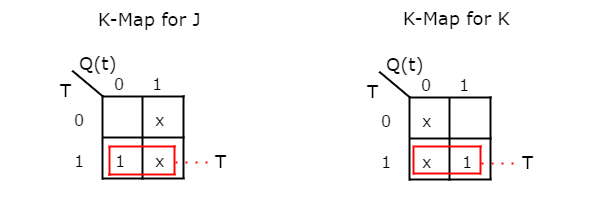
So, we got, J = T & K = T after simplifying. The circuit diagram of T flip-flop is shown in the following figure.
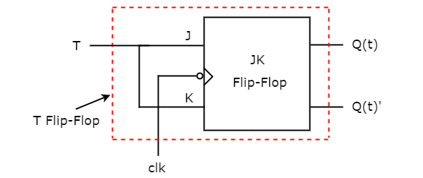
This circuit consists of JK flip-flop only. It doesn’t require any other gates. Just connect the same input T to both J & K. So, the overall circuit has single input, T and two outputs Q(t) & Q(t)’. Hence, it is a T flip-flop. Similarly, you can do other two conversions.
T Flip-Flop to other Flip-Flop Conversions
Following are the three possible conversions of T flip-flop to other flip-flops.
- T flip-flop to D flip-flop
- T flip-flop to SR flip-flop
- T flip-flop to JK flip-flop
T flip-flop to D flip-flop conversion
Here, the given flip-flop is T flip-flop and the desired flip-flop is D flip-flop. Therefore, consider the characteristic table of D flip-flop and write down the excitation values of T flip-flop for each combination of present state and next state values. The following table shows the characteristic table of D flip-flop along with the excitation input of T flip-flop.
| D flip-flop input | Present State | Next State | T flip-flop input | |
|---|---|---|---|---|
| D | Q(t) | Q(t + 1) | T | |
| 0 | 0 | 0 | 0 | |
| 0 | 1 | 0 | 1 | |
| 1 | 0 | 1 | 1 | |
| 1 | 1 | 1 | 0 | |
From the above table, we can directly write the Boolean function of T as below.
So, we require a two input Exclusive-OR gate along with T flip-flop. The circuit diagram of D flip-flop is shown in the following figure.
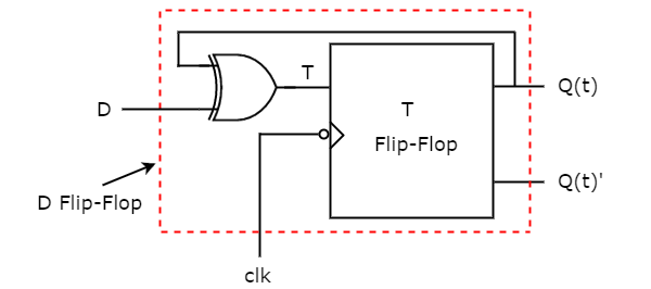
This circuit consists of T flip-flop and an Exclusive-OR gate. This Exclusive-OR gate produces an output, which is Ex-OR of D and Q(t). So, the overall circuit has single input, D and two outputs Q(t) & Q(t)’. Hence, it is a D flip-flop. Similarly, you can do other two conversions.
Comments
Post a Comment