
In previous chapter, we discussed about Latches. Those are the basic building blocks of flip-flops. We can implement flip-flops in two methods.
In first method, cascade two latches in such a way that the first latch is enabled for every positive clock pulse and second latch is enabled for every negative clock pulse. So that the combination of these two latches become a flip-flop.
In second method, we can directly implement the flip-flop, which is edge sensitive. In this chapter, let us discuss the following flip-flops using second method.
- SR Flip-Flop
- D Flip-Flop
- JK Flip-Flop
- T Flip-Flop
SR Flip-Flop
SR flip-flop operates with only positive clock transitions or negative clock transitions. Whereas, SR latch operates with enable signal. The circuit diagramof SR flip-flop is shown in the following figure.
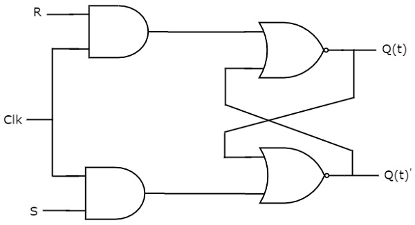
This circuit has two inputs S & R and two outputs Q(t) & Q(t)’. The operation of SR flipflop is similar to SR Latch. But, this flip-flop affects the outputs only when positive transition of the clock signal is applied instead of active enable.
The following table shows the state table of SR flip-flop.
| S | R | Q(t + 1) |
|---|---|---|
| 0 | 0 | Q(t) |
| 0 | 1 | 0 |
| 1 | 0 | 1 |
| 1 | 1 | - |
Here, Q(t) & Q(t + 1) are present state & next state respectively. So, SR flip-flop can be used for one of these three functions such as Hold, Reset & Set based on the input conditions, when positive transition of clock signal is applied. The following table shows the characteristic table of SR flip-flop.
| Present Inputs | Present State | Next State | |
|---|---|---|---|
| S | R | Q(t) | Q(t + 1) |
| 0 | 0 | 0 | 0 |
| 0 | 0 | 1 | 1 |
| 0 | 1 | 0 | 0 |
| 0 | 1 | 1 | 0 |
| 1 | 0 | 0 | 1 |
| 1 | 0 | 1 | 1 |
| 1 | 1 | 0 | x |
| 1 | 1 | 1 | x |
By using three variable K-Map, we can get the simplified expression for next state, Q(t + 1). The three variable K-Map for next state, Q(t + 1) is shown in the following figure.
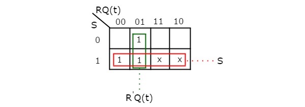
The maximum possible groupings of adjacent ones are already shown in the figure. Therefore, the simplified expression for next state Q(t + 1) is
D Flip-Flop
D flip-flop operates with only positive clock transitions or negative clock transitions. Whereas, D latch operates with enable signal. That means, the output of D flip-flop is insensitive to the changes in the input, D except for active transition of the clock signal. The circuit diagram of D flip-flop is shown in the following figure.
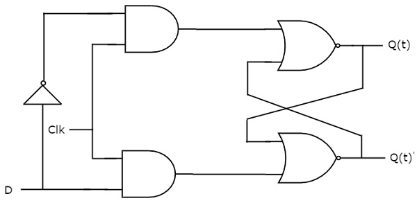
This circuit has single input D and two outputs Q(t) & Q(t)’. The operation of D flip-flop is similar to D Latch. But, this flip-flop affects the outputs only when positive transition of the clock signal is applied instead of active enable.
The following table shows the state table of D flip-flop.
| D | Q(t + 1) |
|---|---|
| 0 | 0 |
| 0 | 1 |
Therefore, D flip-flop always Hold the information, which is available on data input, D of earlier positive transition of clock signal. From the above state table, we can directly write the next state equation as
Q(t + 1) = D
Next state of D flip-flop is always equal to data input, D for every positive transition of the clock signal. Hence, D flip-flops can be used in registers, shift registers and some of the counters.
JK Flip-Flop
JK flip-flop is the modified version of SR flip-flop. It operates with only positive clock transitions or negative clock transitions. The circuit diagram of JK flip-flop is shown in the following figure.
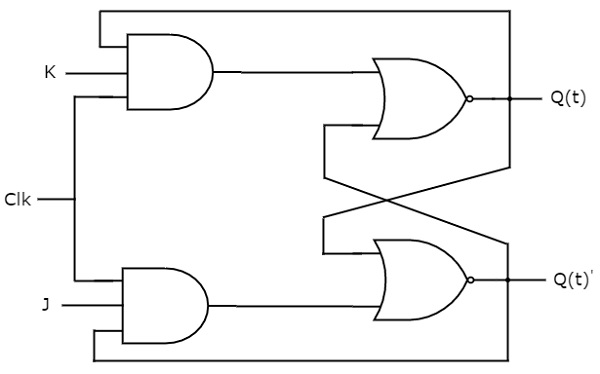
This circuit has two inputs J & K and two outputs Q(t) & Q(t)’. The operation of JK flip-flop is similar to SR flip-flop. Here, we considered the inputs of SR flip-flop as S = J Q(t)’ and R = KQ(t) in order to utilize the modified SR flip-flop for 4 combinations of inputs.
The following table shows the state table of JK flip-flop.
| J | K | Q(t + 1) |
|---|---|---|
| 0 | 0 | Q(t) |
| 0 | 1 | 0 |
| 1 | 0 | 1 |
| 1 | 1 | Q(t)' |
Here, Q(t) & Q(t + 1) are present state & next state respectively. So, JK flip-flop can be used for one of these four functions such as Hold, Reset, Set & Complement of present state based on the input conditions, when positive transition of clock signal is applied. The following table shows the characteristic table of JK flip-flop.
| Present Inputs | Present State | Next State | |
|---|---|---|---|
| J | K | Q(t) | Q(t+1) |
| 0 | 0 | 0 | 0 |
| 0 | 0 | 1 | 1 |
| 0 | 1 | 0 | 0 |
| 0 | 1 | 1 | 0 |
| 1 | 0 | 0 | 1 |
| 1 | 0 | 1 | 1 |
| 1 | 1 | 0 | 1 |
| 1 | 1 | 1 | 0 |
By using three variable K-Map, we can get the simplified expression for next state, Q(t + 1). Three variable K-Map for next state, Q(t + 1) is shown in the following figure.
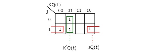
The maximum possible groupings of adjacent ones are already shown in the figure. Therefore, the simplified expression for next state Q(t+1) is
T Flip-Flop
T flip-flop is the simplified version of JK flip-flop. It is obtained by connecting the same input ‘T’ to both inputs of JK flip-flop. It operates with only positive clock transitions or negative clock transitions. The circuit diagram of T flip-flop is shown in the following figure.
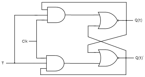
This circuit has single input T and two outputs Q(t) & Q(t)’. The operation of T flip-flop is same as that of JK flip-flop. Here, we considered the inputs of JK flip-flop as J = T and K = T in order to utilize the modified JK flip-flop for 2 combinations of inputs. So, we eliminated the other two combinations of J & K, for which those two values are complement to each other in T flip-flop.
The following table shows the state table of T flip-flop.
| D | Q(t + 1) |
|---|---|
| 0 | Q(t) |
| 1 | Q(t)’ |
Here, Q(t) & Q(t + 1) are present state & next state respectively. So, T flip-flop can be used for one of these two functions such as Hold, & Complement of present state based on the input conditions, when positive transition of clock signal is applied. The following table shows the characteristic table of T flip-flop.
| Inputs | Present State | Next State |
|---|---|---|
| T | Q(t) | Q(t + 1) |
| 0 | 0 | 0 |
| 0 | 1 | 1 |
| 1 | 0 | 1 |
| 1 | 1 | 0 |
From the above characteristic table, we can directly write the next state equation as
The output of T flip-flop always toggles for every positive transition of the clock signal, when input T remains at logic High (1). Hence, T flip-flop can be used in counters.
In this chapter, we implemented various flip-flops by providing the cross coupling between NOR gates. Similarly, you can implement these flip-flops by using NAND gates.
Comments
Post a Comment